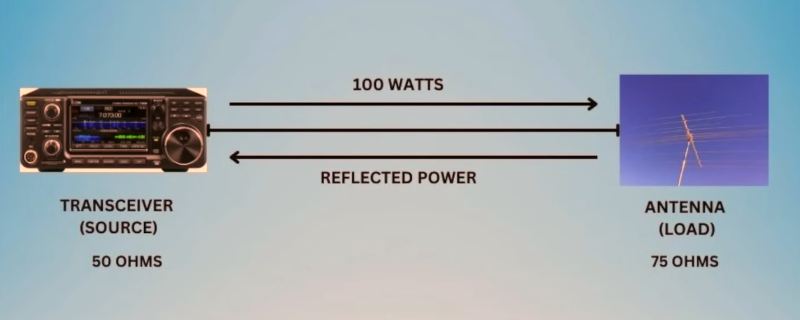
If you are involved in any sort of radio transmission, you probably have at least heard of SWR or standing wave ratio. Most transmitters can measure it these days and most ham radio operators have tuners that measure it, also. But what are you measuring? [KI8R] points out that if your coax has loss — and what coax doesn’t? — you are probably getting an artificially low reading by measuring at the transmitter.
The reason is that most common SWR-measuring instruments pick up voltage. If you measure, for example, 10V going out and 1V going back, you’d assume some SWR from that. But suppose your coax loses half the voltage (just to make an obvious example; if your coax loses half the voltage, you need new coax).
Now, you really have 5V getting to your antenna, and it returns 2V. The loss will affect the return voltage just like the forward voltage. Reflecting 2V from 5 is a very different proposition from reflecting 1V out of 10!
On the other hand, as [KI8R] points out, SWR isn’t everything. In the old days, you’d load your transmitter’s finals into just about anything. Now, solid-state rigs expect to drive a low SWR, or they will crank down the power to prevent the reverse voltage from damaging them.
Overall, it is a good talk about a subject that is often taken for granted. Of course, with cheap VNAs, you can easily measure SWR right at the antenna, often with disappointing results. If you have trouble visualizing standing waves, we know someone who can help.
Here’s the thing about radio signals. There is wild and interesting stuff just getting beamed around all over the place. Phrased another way, there are beautiful signals everywhere for those with ears to listen. We go about our lives oblivious to most of them, but some dedicate their time to teasing out and capturing these transmissions.
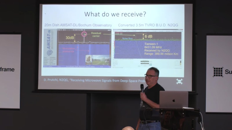
David Prutchi is one such person. He’s a ham radio enthusiast that dabbles in receiving microwave signals sent from probes in deep space. What’s even better is that he came down to Supercon 2023 to tell us all about how it’s done!
Space Calling
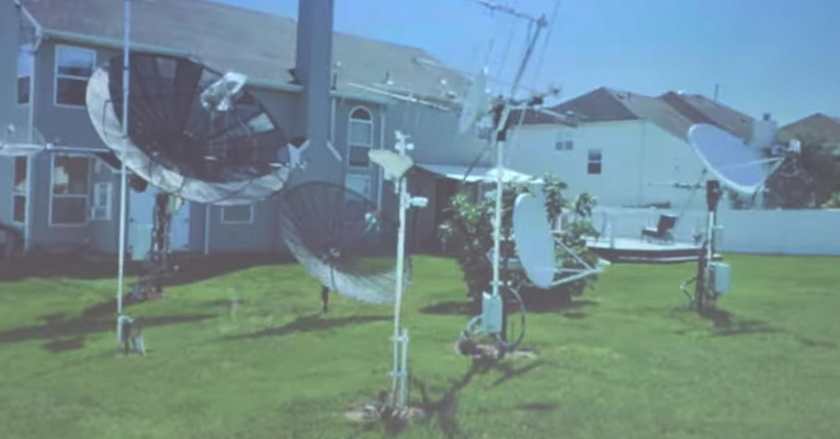
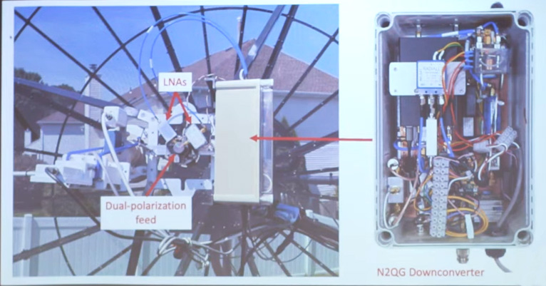
David’s home setup is pretty rad.
David notes that he’s not the only ham out there doing this. He celebrates the small community of passionate hams that specialize in capturing signals directly from far-off spacecraft. As one of these dedicated enthusiasts, he gives us a look at his backyard setup—full of multiple parabolic dishes for getting the best possible reception when it comes to signals sent from so far away. They’re a damn sight smaller than NASA’s deep space network (DSN) 70-meter dish antennas, but they can still do the job. He likens trying to find distant space signals as to “watching grass grow”—sitting in front of a monitor, waiting for a tiny little spike to show up on a spectrogram.
Listening to signals from far away is hard. You want the biggest, best antenna you can get.
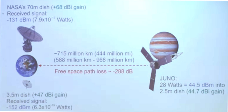
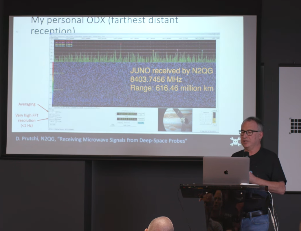
The challenge of receiving these signals comes down to simple numbers. David explains that a spacecraft like JUNO emits 28 watts into a 2.5-meter dish, which comes out to roughly 44.5 dBm of signal with a 44.7 dBi gain antenna. The problem is one of distance—it sits at around 715 million kilometers away on its mission to visit Jupiter. That comes with a path loss of around -288 dB. NASA’s 70-meter dish gets them 68 dBi gain on the receive side, which gets them a received signal strength around -131 dBm. To transmit in return, they transmit around the 50-60 kW range using the same antenna. David’s setup is altogether more humble, with a 3.5-meter dish getting him 47 dBi gain. His received signal strength is much lower, around -152 dBm.
His equipment limits what he can actually get from these distant spacecraft. National space agencies can get full signal from their dishes in the tens-of-meters in diameter, sidebands and all. His smaller setup is often just enough to get some of the residual carrier showing up in the spectrogram. Given he’s not getting full signal, how does he know what he’s receiving is the real deal? It comes down to checking the doppler shift in the spectrogram, which is readily apparent for spacecraft signals. He also references the movie Contact, noting that the techniques in that film were valid. If you move your antenna to point away from the suspected spacecraft, the signal should go away. If it doesn’t, it might be that you’re picking up local interference instead.
THIS. IS. JUST. AWESOME. !!!
This is video decoded from the 8455MHz high rate downlink @uhf_satcom received yesterday. All the work on the decoder and data analysis really paid off in the end!
Video shows solar panel of Chang’e-5 glistening in the sun and dust floating around. pic.twitter.com/FKc92kgskl
Some hobbyists have been able to decode video feeds from spacecraft downlinks.
Working at microwave frequencies requires the proper equipment. You’ll want a downconverter mounted as close to your antenna as possible if you’re working in X-Band.
However, demodulating and decoding full spacecraft signals at home is sometimes possible—generally when the spacecraft are still close to Earth. Some hobbyists have been able to decode telemetry from various missions, and even video signals from some craft! David shows some examples, noting that SpaceX has since started encrypting its feeds after hobbyists first started decoding them.
David also highlights the communications bands most typically used for deep space communication, and explains how to listen in on them. Most of it goes on in the S-band and X-band frequencies, with long-range activity focused on the higher bands.
David has pulled in some truly distant signals.
Basically, if you want to get involved in this kind of thing, you’re going to want a dish and some kind of software defined radio. If you’re listening in S-band, that’s possibly enough, but if you’re stepping up into X-band, you’ll want a downconverter to step that signal down to a lower frequency range, mounted as close to your dish as possible. This is important as X-band signals get attenuated very quickly in even short cable runs. It’s also generally required to lock your downconverter and radio receiver to some kind of atomic clock source to keep them stable. You’ll also want an antenna rotator to point your dishes accurately, based on data you can source from NASA JPL. As for finding downlink frequencies, he suggests looking at the ITU or the Australian Communication and Media Authority website.
He also covers the techniques of optimizing your setup. He dives into the minutae of pointing antennas at the Sun and Moon to pick up their characteristic noise for calibration purposes. It’s a great way to determine the performance of your antenna and supporting setup. Alternatively, you can use signals from geostationary military satellites to determine how much signal you’re getting—or losing—from your equipment.
Ultimately, if you’ve ever dreamed of listening to distant spacecraft, David’s talk is a great place to start. It’s a primer on the equipment and techniques you need to get started, and he also makes it sound really fun, to boot. It’s high-tech hamming at its best, and there’s more to listen to out there than ever—so get stuck in!
In an age where our gadgets allow us to explore the cosmos, we stumbled upon sounds from a future past: an article on historical signals from Mars. The piece, written by [Paul Gilster] of Centauri Dreams, cites a Times essay published by [Becky Ferreira] of August 20. [Ferreira]’s essay sheds light on a fascinating, if peculiar, chapter in the history of the search for extraterrestrial life.
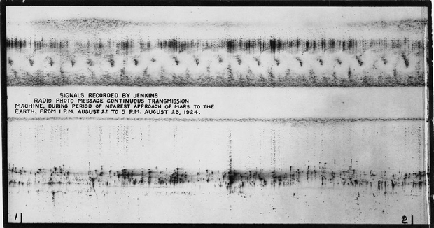
She recounts an event from August 1924 when the U.S. Navy imposed a nationwide radio silence for five minutes each hour to allow observatories to listen for signals from Mars. This initiative aimed to capitalize on the planet’s close alignment with Earth, sparking intrigue and excitement among astronomers and enthusiasts alike.
Amid the technological optimism of the era, a dirigible equipped with radio equipment took to the skies to monitor potential Martian messages. The excitement peaked when a series of dots and dashes captured by the airborne antenna suggested a “crudely drawn face.” Some scientists speculated that this could be a signal from a Martian civilization, igniting a media frenzy. Yet, skeptics, including inventor C. Francis Jenkins, suggested these results were merely a case of radio frequency interference—an early reminder of the challenges we face in discerning genuine signals from the noise of our own planet.
As we tinker with our devices and dream of interstellar communication, the 1924 incident reminds us that the search for extraterrestrial intelligence is a blend of curiosity, creativity, and, often, misinterpretation.
If you need an amplifier, [Hans Rosenberg] has some advice. Don’t design your own; grab cheap and tiny RF amplifier modules and put them on a PCB that fits your needs. These are the grandchildren of the old mini circuits modules that were popular among hams and RF experimenters decades ago. However, these are cheap, simple, and tiny.
You only need a handful of components to make them work, and [Hans] shows you how to make the selection and what you need to think about when laying out the PC board. Check out the video below for a very detailed deep dive.
To get the best performance, the PCB layout is at least as important as the components. [Hans] shows what’s important and how to best work out what you need using some online calculators.
Using a NanoVNA and a USB spectrum analyzer, [Hans] makes some measurements on the devices using different components, which is very instructive. The measurements lined up fairly well with the theory, and you can see the effects of changing key components in the design.
For as useful as computers are in the modern ham shack, they also tend to be a strong source of unwanted radio frequency interference. Common wisdom says applying a few ferrite beads to things like Ethernet cables will help, but does that really work?
It surely appears to, for the most part at least, according to experiments done by [Ham Radio DX]. With a particular interest in lowering the noise floor for operations in the 2-meter band, his test setup consisted of a NanoVNA and a simple chunk of wire standing in for the twisted-pair conductors inside an Ethernet cable. The NanoVNA was set to sweep across the entire HF band and up into the VHF; various styles of ferrite were then added to the conductor and the frequency response observed. Simply clamping a single ferrite on the wire helped a little, with marginal improvement seen by adding one or two more ferrites. A much more dramatic improvement was seen by looping the conductor back through the ferrite for an additional turn, with diminishing returns at higher frequencies as more turns were added. The best performance seemed to come from two ferrites with two turns each, which gave 17 dB of suppression across the tested bandwidth.
The question then becomes: How do the ferrites affect Ethernet performance? [Ham Radio DX] tested that too, and it looks like good news there. Using a 30-meter-long Cat 5 cable and testing file transfer speed with iPerf, he found no measurable effect on throughput no matter what ferrites he added to the cable. In fact, some ferrites actually seemed to boost the file transfer speed slightly.
Ferrite beads for RFI suppression are nothing new, of course, but it’s nice to see a real-world test that tells you both how and where to apply them. The fact that you won’t be borking your connection is nice to know, too. Then again, maybe it’s not your Ethernet that’s causing the problem, in which case maybe you’ll need a little help from a thunderstorm to track down the issue.
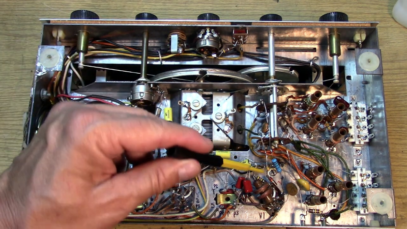
[MIKROWAVE1] claims he’s not a radio repair guy, but he agreed to look at a malfunctioning Hallicrafters S-120 shortwave receiver. He lets us watch as he tries to get it in shape in the video below. You’ll see that one of his subscribers had done a great job restoring the radio, but it just didn’t work well.
Everything looked great including the restored parts, so it was a mystery why things wouldn’t work. However, every voltage measured was about 20V too low. Turns out that the series fuse resistor had changed value and was dropping too much voltage.
That was an easy fix and got three of the radio’s four bands working. The fourth band had some problems. Fixing some grounding helped, but the converter tube was weak and a new replacement made it work much better.
There were some other minor issues, but in the end, the radio was back to its original glory. We have to warn you that restoring old radios can be addictive. The good news is, thanks to the Internet, you don’t have to figure it all out yourself or find a local expert who will take an apprentice. Hallicrafters was a huge name in the radio business after World War II, and, for that matter, during the war, too.
The United States and a few other countries have an astounding array of homeowners’ associations (HOAs), local organizations that exert an inordinate influence on what homeowners can and can’t do with their properties, with enforcement mechanisms up to foreclosure. In the worst cases they can get fussy about things like the shade of brown a homeowner can paint their mailbox post, so you can imagine the problems they’d have with things like ham radio antennas. [Bob] aka [KD4BMG] has been working on tuning up his rain gutters to use as “stealth” antennas to avoid any conflicts with his HOA.
With the right antenna tuner, essentially any piece of metal can be connected to a radio and used as an antenna. There are a few things that improve that antenna’s performance, though. [Bob] already has an inconspicuous coax connector mounted on the outside of his house with an antenna tuner that normally runs his end-fed sloper antenna, which also looks like it includes a fairly robust ground wire running around his home. All of this is coincidentally located right beside a metal downspout, so all this took to start making contacts was to run a short wire from the tuner to the gutter system.
With the tuner doing a bit of work, [Bob] was able to make plenty of contacts from 10 to 80 meters, with most of the contacts in the 20 – 30 meter bands. Although the FCC in the US technically forbids HOAs from restricting reasonable antennas, if you’d rather not get on the bad side of your least favorite neighbors there are a few other projects from [Bob] to hide your gear.
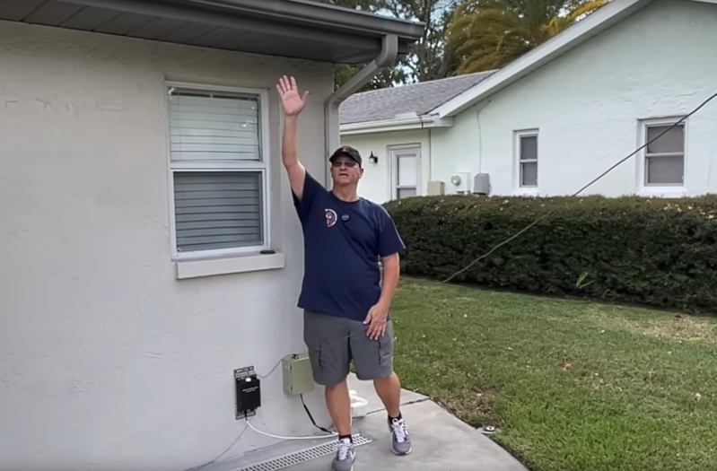
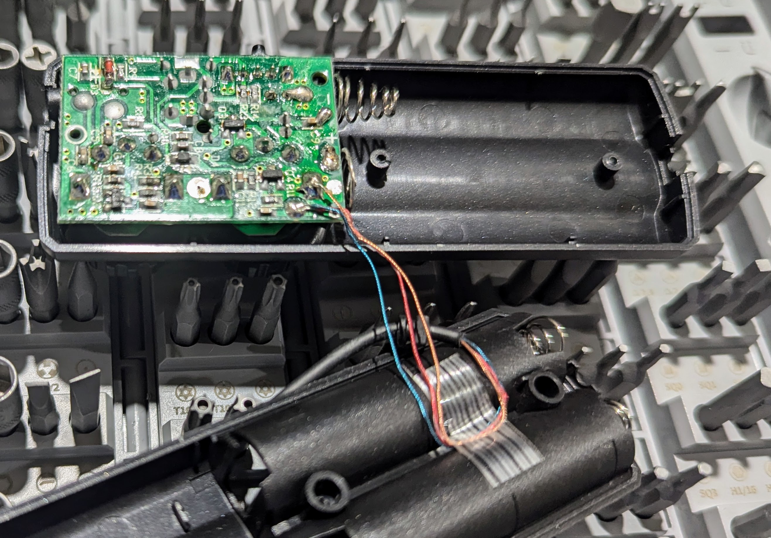
It is one of Murphy’s laws, we think, that you can’t get great things when you need them. Back in the heyday of shortwave broadcasting, any of us would have given a week’s pay for even a low-end receiver today. Digital display? Memory? Digital filtering? These days, you have radios, and they aren’t terribly expensive, but there isn’t much to listen to. Making matters worse, it isn’t easy these days to string wires around in your neighborhood for a variety of reasons. Maybe you don’t have a yard, or you have deed restrictions, or your yard lacks suitable space or locations. This problem is so common that there are a crop of indoor antennas that seem attractive. Since I don’t often tune in shortwave and I don’t want to have to reset my antenna after every storm, I decided to look at the Tecsun AN-48X along with a YouLoop clone from China. Let’s start with the Tecsun.
In the Box
The Tecsun in a more or less diamond shape
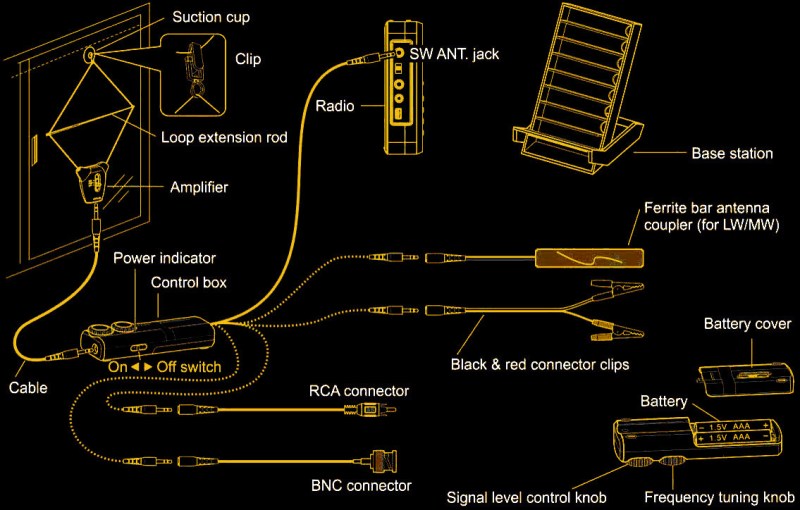
The antenna is not terribly cheap at about $50 or so, but there’s a lot in the box. The business end looks like something you’d wear around your neck. A small box has a switch for three bands — LW, AM, and SW. the two wires coming out of that box form a loop. You can stick the loop to something using a suction cup or a hook. There’s also a little bar that looks like a standard telescoping antenna but it has two plastic clips on the end. You use this to form the loop into a diamond shape with the telescoping rod about halfway.
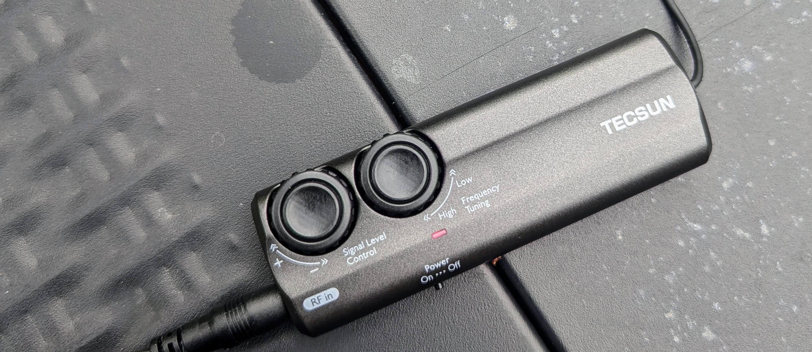
At the bottom of the box with the switch is a standard 1/8″ jack. A cable connects that jack to a similar jack on the control unit which is about the size of a large pack of gum and has two AAA batteries inside. That box has a switch, two knobs, and a pigtail with another 1/8″ jack.
If your radio takes a 1/8″ plug for an antenna, that’s where you connect it. If it doesn’t, you have a few options. The box contains pigtails that convert the plug to BNC, RCA, alligator clips, or a ferrite bar that can couple to a radio’s internal antenna. You probably need SMA for a modern radio, so you’ll need an adapter. There’s also a plastic stand that can hold your radio and the ferrite bar if you are using it.
The knobs on the control box control the gain and tune the frequency of the antenna. Other than the switch close to the loop, all the other controls are on the control box, which stays close to your radio. So, as long as you don’t care about jumping between LW, AM, and SW, you don’t need to access the loop part during operation.
A Few Tests
I decided to try the antenna at a few different times a day in a few different locations. I used an old portable DAK shortwave receiver and also a more modern SDR receiver.
The Tecsun control box.
For the first test, I hung the loop on my upstairs stair rail and let the cable drop down to the first floor. During the day, WWV was barely audible, and there was little else to hear outside of noise. Granted, this was indoors. The signal level control didn’t seem to do much. The tuning frequency knob reminded me of a regenerative receiver control. You could hear the device oscillate, and just past the oscillation, you’d get the best signal. It made me wonder if the inner circuit was, in fact, a regenerative amplifier.
The portable shortwave uses a regular jack, but for the Malachite, I had to use a BNC to SMA adapter. Neither radio could pull much out. Nighttime reception was a little better, but not much.
The Great Outdoors
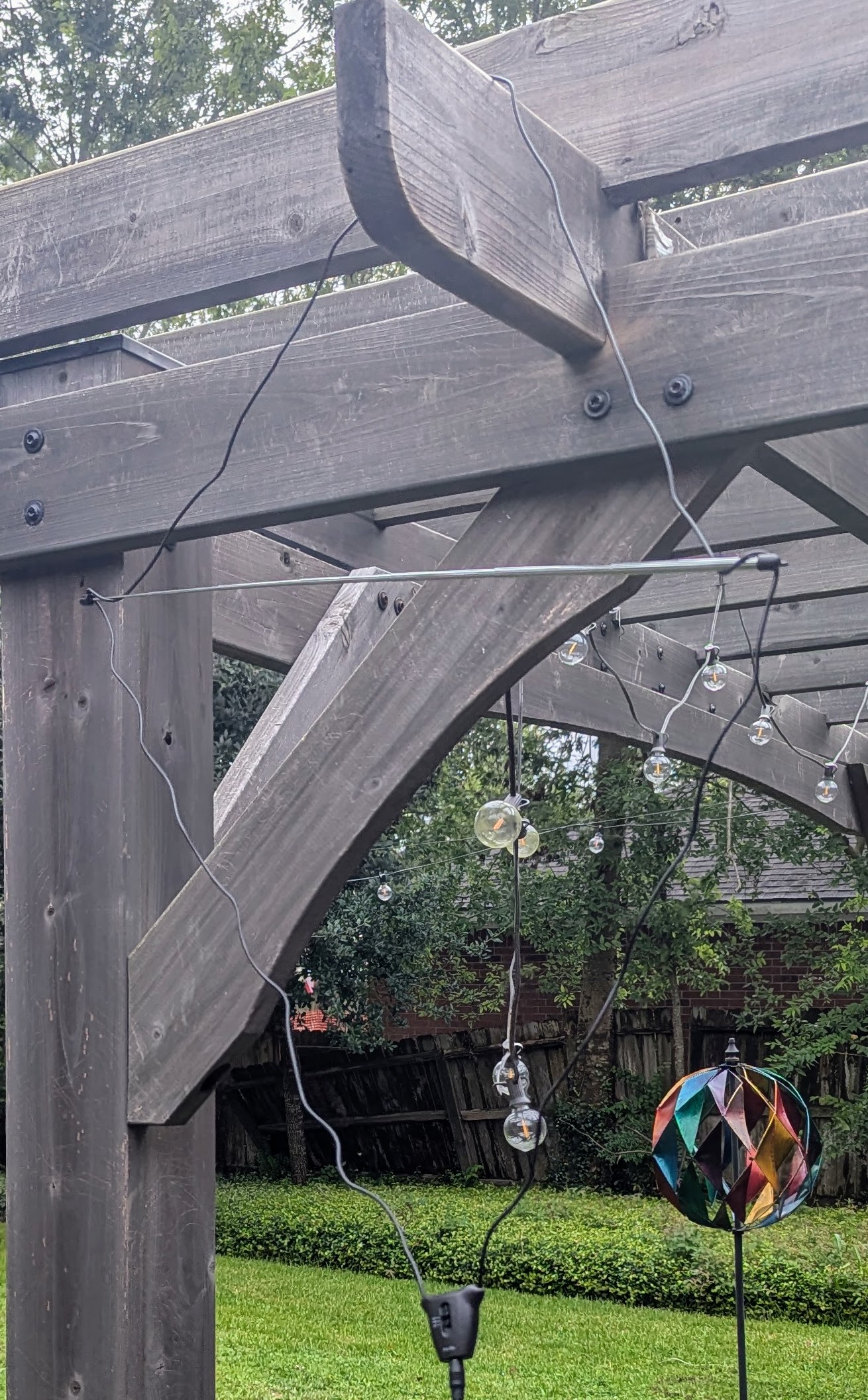
Unsurprisingly, the device worked a little better outdoors. I hung it from an exposed beam on a pergola, and at night, there were a few fairly clear signals. During the daylight hours, WWV was elusive, but the Voice of America and Radio Havana — not too far from Houston — were easy to copy, especially if you understand French. I even managed to catch a few faint snags of WWVH.
The video below shows a few audio clips of the results. Forgive the outdoor glare on the screen in the first clip. I omitted the clips with music that YouTube might flag, but you get the idea.
I also tested a YouLoop clone. This worked almost as well as the Techsun, but not quite as well. However, there was nothing to fidget with on the frequency.
The YouLoop
The YouLoop has an interesting idea. It uses coax for the loop and configures it like a Mobius strip so that it is kind of, an infinite loop. At the bottom is a balun with three connectors, and at the top is a phase inverter. That sounds fancy, but it really is just a box that connects the inside of one cable to the outside of the other. The antenna came with a powered preamp, although if your radio has a preamp, you probably don’t need it.
It is handy that it just works, and the coax sections are stiff enough to be easy to handle when you want to hang it from a branch, for example. However, it also doesn’t pack down as tightly, and the boxes are metal, which adds to the weight but is probably better for shielding.
Signals on this loop were almost always lower in volume than the same signal from the Tecsun, even with the preamp. On the other hand, if you don’t need the preamp, this antenna takes no batteries. It is simple enough that you can try it and see if you like it without a major investment.
Observations
The Tecsun control board revealed
While the Tecsun is light, I can’t help but wonder if the shielded feedline might not have helped it. For both antennas, having the preamp close up to the feed point might pay off, although maybe some of the wire between the antenna and the control boxes or preamp becomes part of the antenna. It isn’t, after all, a tuned antenna.
The Tecsun’s control box frequency knob is maddeningly sensitive, but it does seem to help things. Inside the box is a tiny PCB, and I didn’t find any online schematics.
Should you run out and get either of these antennas? If you have other options, probably not. But if you need something, both of them are better than nothing.
A QSL Card from Radio Moscow probably got many 14-year-olds on government watch lists. (Public domain)
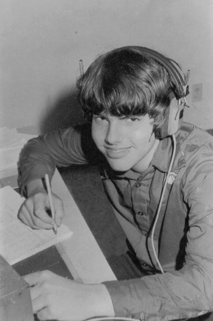
Between World War II and Y2K, shortwave listening was quite an education. With a simple receiver, you could listen to the world. Some of it, of course, was entertainment, and much of it was propaganda of one sort or another. But you could learn a lot. Kids with shortwave radios always did great in geography. Getting the news from a different perspective is often illuminating, too. Learning about other cultures and people in such a direct way is priceless. Getting a QSL card in the mail from a faraway land seemed very exciting back then.
Today, the shortwave landscape is a mere shadow of itself. According to a Wikipedia page, there are 235 active shortwave broadcasters from a list of 414, so nearly half are defunct. Not only are there many “dead” shortwave outlets, but many of the ones that are left are either not aimed at the world market or serve a niche group of listeners.
You can argue that with the Internet, you don’t need radio, and that’s probably correct in some ways but misses a few important points. Indeed, many broadcasters still exist as streaming stations or a mix of radio and streaming. I have to admit I listen to the BBC often but rarely on the air. My computer or phone plays it in crystal clarity 24 hours a day.
A future Hackaday author in front of an Eico shortwave radio
So, while a 14-year-old in 1975 might be hunched over a radio wearing headphones, straining to hear NHK World Radio, these days, they are likely surfing the popular social media site of the week. You could easily argue that content on YouTube, Instagram, and the like can come from all over the world, so what’s the problem?
The problem is information overload. Faced with a shortwave radio, there were a limited number of options available. What’s more, only a small part of the band might be “open” at any given time. It isn’t like the radio could play games or — unless you were a ham — allow you to chat with your friends. So you found radio stations from Germany to South Africa. From China and Russia, to Canada and Mexico. You knew the capital of Albania. You learned a little Dutch from Radio Nederlands.
Is there an answer? Probably not. Radio isn’t coming back, barring an apocalyptic event. Sure, you can listen to the BBC on your computer, but you probably won’t. You can even listen to a radio over the network, but that isn’t going to draw in people who aren’t already interested in radio, even if it really looks like a radio.
If you made a website with radio stations of the world, would people use it? Something like a software version of this globe or a “world service” version of RadioGarden. Probably not.
Do you listen to shortwave radio? If so, what are you listening to? Do you listen to “world services” at all? Tell us in the comments. Many careers were launched by finding a shortwave radio under the Christmas tree at just the right age. When Internet access is compromised, there’s still no substitute for real radios. If you want to listen to some of those vintage programs, they are — unsurprisingly — on the Internet.
When we first spotted the article about a one-transistor amateur radio transceiver, we were sure it was a misprint. We’ve seen a lot of simple low-power receivers using a single transistor, and a fair number of one-transistor transmitters. But both in one package with only a single active component? Curiosity piqued.
It turns out that [Ciprian Popica (YO6DXE)]’s design is exactly what it says on the label, and it’s pretty cool to boot. The design is an improvement on a one-transistor transceiver called “El Pititico” and is very petite indeed. The BOM has only about fifteen parts including a 2N2222 used as a crystal-controlled oscillator for both the transmitter and the direct-conversion receiver, along with a handful of passives and a coupe of hand-wound toroidal inductors. There’s no on-board audio section, so you’ll have to provide an external amplifier to hear the signals; some might say this is cheating a bit from the “one transistor” thing, but we’ll allow it. Oh, and there’s a catch — you have to learn Morse code, since this is a CW-only transmitter.
As for construction, [Ciprian] provides a nice PCB layout, but the video below seems to show a more traditional “ugly style” build, which we always appreciate. The board lives in a wooden box small enough to get lost in a pocket. The transceiver draws about 1.5 mA while receiving and puts out a fairly powerful 500 mW signal, which is fairly high in the QRP world. [Ciprian] reports having milked a full watt out of it with some modifications, but that kind of pushes the transistor into Magic Smoke territory. The signal is a bit chirpy, too, but not too bad.
We love minimalist builds like these; they always have us sizing up our junk bin and wishing we were better stocked on crystals and toroids. It might be good to actually buckle down and learn Morse too.