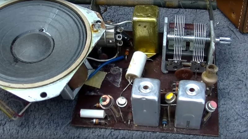
Surplus Syringes Make Satisfactory Tuner For Amateur Radio Experimentation

Amateur Radio as a hobby has a long history of encouraging experimentation using whatever one might have on hand. When [Tom Essenpreis] wanted to use his 14 MHz antenna outside of its designed frequency range, he knew he’d need an impedance matching circuit. The most common type is an L-Match circuit which uses a variable capacitor and a variable inductor to adjust the usable frequency range (resonance) of an antenna. While inefficient in some specific configurations, they excel at bridging the gap between the 50 ohm impedance of the radio and the unknown impedance of an antenna.

No doubt raiding his junk box for parts, [Tom] hacked together a variable capacitor and inductor using ferrite rods from AM radios, hot glue, magnet wire, copper tape, and some surplus 60ml syringes. You can see that he ground out the center of the plunger to make room for ferrite rods. Winding the outside of the syringe with magnet wire, the alignment of the ferrite can be adjusted via the plunger, changing the characteristics of the element to tune the circuit. [Tom] reports that he was able to make an on-air contact using his newly made tuner, and we’re sure he enjoyed putting his improvised equipment to use.

If Amateur Radio isn’t your thing, then maybe we can entice you with this syringe based rocket, syringe actuated 3D printed drill press, or vacuum syringe powered dragster. Have your own hack to share? By all means, submit it to the Tip Line!

A Cheap Dipole Antenna From An Extension Cord

Dipoles are a classic builder’s antenna, after all they are usually little more than two pieces of wire and a feedline. But as [Rob] shows us in the video below, there are a few things to consider.

The first thing is where to get the wire. A damaged extension cord donated the wire. That’s actually an interesting idea because you get multiple wires the same length inside the extension cord. Of course, it is easy to just pull the conductors out of the extension cord, but how do you feed it? A small balun converts the unbalanced feed line into a balanced connection for the antenna. Although the title says “free dipole” this balun is commercial and probably cost something unless you happen to already have one. However, building a balun isn’t all that tricky, either if you happen to have a ferrite toroid.

If you want to transmit, you’ll probably need a little different arrangement, but for receiving this will definitely get the job done. A tuner would make life easier.

Even though this is technically a dipole, without tuning it is more of a random wire. However, it works and with antenna analyzers now common gear, it would be easy to shorten the dipole down to any band you wanted.

Of course, in the mechanical world, they say if you can’t make it exact, make it adjustable. If you are looking for cheap station gear, there’s always the $50 ham, otherwise known as [Dan Maloney].

P

New Video Series: Learning Antenna Basics With Karen Rucker

We don’t normally embrace the supernatural here at Hackaday, but when the topic turns to the radio frequency world, Arthur C. Clarke’s maxim about sufficiently advanced technology being akin to magic pretty much works for us. In the RF realm, the rules of electricity, at least the basic ones, don’t seem to apply, or if they do apply, it’s often with a, “Yeah, but…” caveat that’s sometimes hard to get one’s head around.

Perhaps nowhere does the RF world seem more magical than in antenna design. Sure, an antenna can be as simple as a straight piece or two of wire, but even in their simplest embodiments, antennas belie a complexity that can really be daunting to newbie and vet alike. That’s why we were happy to recently host Karen Rucker’s Introduction to Antenna Basics course as part of Hackaday U.

The class was held over a five-week period starting back in May, and we’ve just posted the edited videos for everyone to enjoy. The class is lead by Karen Rucker, an RF engineer specializing in antenna designs for spacecraft who clearly knows her business. I’ve watched the first video of the series and so far and really enjoy Karen’s style and the material she has chosen to highlight; just the bit about antenna polarization and why circular polarization makes sense for space communications was really useful. I’m keen to dig into the rest of the series playlist soon.

The 2021 session of Hackaday U may be wrapped up now, but fear not — there’s plenty of material available to look over and learn from. Head over to the course list on Hackaday.io, pick something that strikes your fancy, and let the learning begin!


P

Some Of The Many Ways To Build AM Transmitters And Receivers

AM radios are relatively simple devices, and building one is a good way to start exploring the world of radio communications. [GreatScott] does exactly this in the video after the break, building both a transmitter and receiver.

At the most basic level, AM radio works by generating a carrier wave with an oscillator, and then modulating the amplitude with an audio signal. Around these parts, the venerable 555 timer is always brought up whenever things get to oscillating; so you’ll no doubt be happy to see [GreatScott] decided to give it a shot for his first experiments, testing two popular 555 transmitter circuits. One uses the control voltage pin to input the audio signal, while the other uses the reset pin. The CV-pin version worked slightly better, but it was still just barely possible to distinguish a voice over a standard commercial AM/FM receiver.

The next attempt was with a XR2206 function generator kit, which worked quite well when combined with a simple microphone amplifier circuit. But this time the receiving side was swapped out, as [GreatScott] built a basic circuit around a TA7642 AM amplifier/demodulator IC, with only six passive components and a hand-wound coil.

There is no shortage of ways to build AM radios, and we’ve covered quite a few over the years. Off course a 555 timer can also be used in a receiver, and building transmitters using only discrete components is quite simple, as demonstrated by the 10-minute transmitter and single transistor transmitter.


P

The $50 Ham: WSPR-ing Around The World

Everybody has a bucket list,  things to be accomplished before the day we eventually wake up on the wrong side of the grass. Many bucket-list items are far more aspirational than realistic; very few of us with “A trip to space” on our lists are going to live to see that fulfilled. And even the more realistic goals, like the trip to Antarctica that’s been on my list for ages, become less and less likely as your life circumstances change — my wife hates the cold.

Luckily, instead of going to Antarctica by myself — and really, what fun would that be? — I’ve recently been getting some of the satisfaction of world travel through amateur radio. The last installment of “The $50 Ham” highlighted weak-signal digital modes using WSJT-X; in that article, I mentioned a little about the Weak Signal Propagation Reporter, or WSPR. It’s that mode that let me test what’s possible with very low-power transmissions, and allowed me to virtually visit six continents including Antarctica and Sweden-by-way-of-Alaska.


Whispers in the Noise

Ask a random amateur radio operator what’s on his or her mind at any given moment and chances are pretty good the answer will be, “How are the bands right now?” That’s shorthand for what the current state of the ionosphere is, which largely determines how well RF signals will bounce off the various layers of charged particles that wrap around the planet. These layers shift and move in diurnal cycles, and undergo longer-term cycles of strengthening and weakening that depend on the cycles of magnetic activity on the Sun.

Assessing the state of the ionosphere and finding out which bands have a path to which points on the globe used to be something that hams had to do by spinning the dial and listening for beacon stations. Beacons are stations that transmit a generally low-power signal from a fixed, know location on a regular schedule. If you can hear the beacon, chances are good that you’ve got a propagation path between you and the general area of the beacon on that frequency.

While beacons are useful, they have their limits. They depend on the kindness of strangers, who devote resources to running and maintaining the beacon station. Beacons are also subject to occasional maintenance outages, so not hearing a beacon you expect does not necessarily mean that you don’t have a path between two points. But perhaps the most limiting aspect of traditional beacons is that they operate on a pull model — you have to sit down at your radio and intentionally tune into the beacon’s frequency and decode what you hear — beacons almost always use continuous wave (CW) mode with Morse code. Add to that the fact that whatever you learn about the propagation paths available to you stays pretty much within your shack, and beacons have limited utility.

WSPR signal by Louis Taber, CC BY-SA 4.0

With those limitations in mind, Joe Taylor (K1JT) began working on a digital mode in 2008 specifically for exploring propagation paths. The protocol was dubbed WSPR, which of course everyone pronounces as “whisper,” which given its capabilities is an apt name indeed. WSPR is a digital mode that employs special digital signal processing algorithms to decode signals with a signal-to-noise ratio (SNR) of -28 dBm in a bandwidth of 2,500 Hz.

When transmitting, WSPR sends a compressed 50-bit message that encodes the station’s callsign, the grid location, and the transmitter power. The message is modulated using frequency-shift keying at a very low bit rate — less than 1.5 baud. This means an entire message with error correction takes almost two full minutes to send. Transmissions are synchronized by the WSPR software to begin one second into each even-numbered minute, making accurate time synchronization essential.

Propagation Made Visual

The shape of things to come — east coast stations are hitting Antarctica on 20 meters, which means I might too in a few hours when the Sun sets over my QTH.

As cool as the WSPR protocol is, the magic of WSPR comes from the “R” part of its name: reporting. This is where WSPR closes the loop that traditional beacons leave open, since WSPR client software can be configured to log any WSPR signals received and decoded by a station to a central database. WSPRnet.org is the place where all the reports go; the site contains a searchable database of all “spots” reported as well as a map that shows current contacts by many, many stations.

The map on WSPRnet is admittedly a bit janky — it’s based on Google Maps, and an error dialog pops up every time you load a new view. There are other visualizations, though, but even with the issues, WSPRnet’s map is a great way to see what propagation paths may be available to you at the current time.

For example, I took a quick peek at the 20-m band just now and found that from my area, I’ve got solid paths to pretty much all of North America. More importantly, I can see that I have no paths into Europe or Asia, and very little to the south into Central and South America. But, by looking at what’s going on with paths on the east coast of the US, where the sun is currently setting and which are actively reaching several stations in and just offshore of Antarctica, I might have a path to the bottom of the planet coming up as the sun sets over me.

Doing My Part

As I mentioned in my first weak-signals article, I’ve currently got WSJT-X running on a Raspberry Pi 4 that I have dedicated to ham radio use. WSJT-X has a built-in WSPR mode, which makes it easy to switch back and forth between exploring possible propagation paths with WSPR and exploiting that information to make actual QSOs using FT8 or one of the other supported modes.

The beauty of using WSJT-X for WSPR work is that it’s basically completely automated. Depending on how you set it up, you can either be a dedicated WSPR receiving and reporting station, or you can choose to also transmit.

When I’m going to be in the shack / office, which is almost always, I set up WSJT-X to transmit on WSPR with a 20% duty cycle — that is, one out of every five two-minute blocks will be dedicated to transmitting. That way, I can do my part contributing to the WSPR map — there generally aren’t many WSPR beacons operating in my part of North Idaho, so I figure this is my way of pitching in. Plus, I get the occasional bonus of nabbing a cool contact, like the aforementioned hit on DP0GVN-1, a German research vessel parked off the coast of Antarctica that I reached on the 30-m band using just five watts.

Sweden, By Way of Alaska

As cool as it is to know you’ve made a solid contact over a path of about 10,000 km on less power than it takes to run an LED light bulb, there’s also a lot to be said for the unusual stations you receive when you leave your WSPR station running. Case in point: the other day I glanced up at WSJT-X and noticed a strange callsign, SA6BSS. After a while of looking at callsigns you get to know which general areas they come from, and I suspected this was a “rare DX” coming from Europe, which is really hard for me to hit with my antenna from the inland Pacific Northwest. A quick lookup on QRZ.com confirmed that SA6BSS is a ham named Mikael Dagman, based in southern Sweden — cool!

I quickly spun up the WSPRnet map and was surprised to see that Mikael’s station was reporting its position as coming from Alaska rather than Sweden. I zoomed in the map a little and found that the signal was coming from a grid hundreds of kilometers south of Unalaska Island in the Aleutians. What in the world would a Swedish ham be doing in the North Pacific in February?

I shot Mikael a quick email about the contact, and he confirmed that I had indeed received a correct position report from his WSPR station, currently floating around the world on a party balloon! Since he released the balloon on Feb 23, it has traveled at around 11,000 meters altitude from Sweden to the Middle East, across Asia, and over the Pacific to just off the coast of Oregon. There it took a hook and headed back out to sea; as I write this it’s heading roughly in the direction of Hawaii.

Literally WSPR-ing around the world — at least halfway so far. SA6BSS launched a balloon carrying a WSPR transmitter on Feb 23 that crossed the Pacific; I copied it when it was south of the Aleutians.

Mikael was kind enough to include a little information on the WSPR transmitter he included on his balloon, which is completely solar-powered and weighs in at only 2.6 grams. The spareness of his design is almost comical — it’s just a GPS module, an ATMega328, and an Si5351 for the transmitter. It’s a perfect example of what can be done on a budget, which is right in line with “The $50 Ham” concept. So naturally, building a lightweight, inexpensive WSPR beacon will be the basis of the next installment in this series.

Web Pages (and More) Via Shortwave

If you are a ham radio operator, the idea of sending pictures and data over voice channels is nothing new. Hams have lots of techniques for doing that and — not so long ago — even most data transmissions were over phone lines. However, now everyone can get in on the game thanks to the cheap availability of software-defined radio. Several commercial shortwave broadcasters are sending encoded data including images and even entire web pages. You can find out more at the Swradiogram website. You can also find step-by-step instructions.

WINB in Pennsylvania and WRMI Florida both have shows that include interspersed data. To play along, you’ll need a decoder like Fldigi or TIVAR. If you don’t have sufficient radio gear, you can probably borrow some from the Internet.


On the face of it, this might seem to be just a geeky hobby, but we can’t help but think that in places where data is censored, radio might be a viable way to send information. Some forward error correction codes and perhaps encryption could be a way to have a data lifeline to those forbidden from free access to the Internet. After all, history is full of stories of secret radio receivers tuned to the BBC or some other radio outlet, or examples of secret messages in broadcasts, such as Radio Swan. If you know Morse code, you might even get a warning about your impending rescue.

Retrotechtacular: Philips Factory Tour, Circa 1930s

Een interessant filmpje (30 min.) over Philips in de jaren ’30 waarin je kunt zien hoe men vacuümbuizen en luidsprekers maakte.

If you’ve got a half-hour or so to spare, you could do worse than this video trip through a Philips factory in the 1930s.

The film is presented without narration, but from the Dutch title cards and the fact that it’s Philips, we gather that this factory of gigantic proportions was somewhere in the Netherlands. In any case, it looks like something right out of [Fritz Lang]’s Metropolis and turned the rawest of materials into finished consumer products.

Much of the film focuses on the making of vacuum tubes; the sheer physicality of the job is what really stands out here. The upper body strength that the glassblowers had to have boggles the mind. Check out the chops — and the soon-to-be very unfashionable mustache — on the glassblower at the 12:00 mark. And it wasn’t just the gents who had mad skills — the fine motor control needed for the delicate assembly of the innards of the tubes, which seems to be mostly staffed by women, is just as impressive. We were also surprised by the amount these manual crafts were assisted by automated systems.

Especially interesting is the section where they build the luidspreker. Without narration or captions, it’s a little hard to tell what’s going on, but it appears that they used an enormous press to form chips of Bakelite into sleek covers for the speakers, which themselves are super-chunky affairs made from scratch in the factory. We’re also treated to assembly of the radios, packaging of finished products, and a group of dockworkers who clearly didn’t read the “Fragile” labels pasted on the boxes.

One can’t help but wonder if these people had the slightest inkling of what was about to sweep over them and the rest of the world. And if they did, would they even begin to comprehend how much the very products that they were making would contribute to both the slaughter of the coming war as well as to the sparing of so many lives? Likely not, but the film is still an interesting glimpse into the creation of an industry, one that relied very much on craftsmanship to get it started.


Circuit Impedance Calculations Without Cumbersome Simulations

Using circuit simulating software like SPICE can be a powerful tool for modeling the behavior of a circuit in the real world. On the other hand, it’s not always necessary to have all of the features of SPICE available all the time, and these programs tend to be quite expensive as well. To that end, [Wes Hileman] noticed an opportunity for a specific, quick method for performing impedance calculations using python without bulky, expensive software and came up with a program which he calls fastZ.

The software works on any network of passive components (resistors, capacitors, and inductors) and the user can specify parallel and series connections using special operators. Not only can the program calculate the combined impedance but it can perform frequency analysis at a specified frequency or graph the frequency response over a wide range of frequencies. It’s also running in python which makes it as simple as importing any other python package, and is also easy to implement in any other python program compared to building a simulation and hoping for the best.

If you find yourself regularly drawing Bode plots or trying to cobble together a circuit simulation to work with your python code, this sort of solution is a great way to save a lot of headache. It is possible to get the a piece of software like SPICE to to work together with other python programs though, often with some pretty interesting results.

Capstan Winch Central To This All-Band Adjustable Dipole Antenna

The perfect antenna is the holy grail of amateur radio. But antenna tuning is a game of inches, and since the optimum length of an antenna depends on the frequency it’s used on, the mere act of spinning the dial means that every antenna design is a compromise. Or perhaps not, if you build this infinitely adjustable capstan-winch dipole antenna.

Dipoles are generally built to resonate around the center frequency of one band, and with allocations ranging almost from “DC to daylight”, hams often end up with a forest of dipoles. [AD0MZ]’s adjustable dipole solves that problem, making the antenna usable from the 80-meter band down to 10 meters. To accomplish this feat it uses something familiar to any sailor: a capstan winch.

The feedpoint of the antenna contains a pair of 3D-printed drums, each wound with a loop of tinned 18-gauge antenna wire attached to some Dacron cord. These make up the adjustable-length elements of the antenna, which are strung through pulleys suspended in trees about 40 meters apart. Inside the feedpoint enclosure are brushes from an electric drill to connect the elements to a 1:1 balun and a stepper motor to run the winch. As the wire pays out of one spool, the Dacron cord is taken up by the other; the same thing happens on the other side of the antenna, resulting in a balanced configuration.

We think this is a really clever design that should make many a ham happy across the bands. We even see how this could be adapted to other antenna configurations, like the end-fed halfwave we recently featured in our “$50 Ham” series.

Teardown of a quartz crystal oscillator and the tiny IC inside

Inside the oscillator package, showing the components mounted on the ceramic substrate.The quartz oscillator is an important electronic circuit, providing highly-accurate timing signals at a low cost. A quartz crystal has the special property of piezoelectricity, changing its electrical properties as it vibrates. Since a crystal can be cut to vibrate at a very precise frequency, quartz oscillators are useful for many applications. Quartz oscillators were introduced in the 1920s and provided accurate frequencies for radio stations. Wristwatches were revolutionized in the 1970s by the use of highly-accurate quartz oscillators. Computers use quartz oscillators to generate their clock signals, from ENIAC in the 1940s to modern computers.1

A quartz crystal requires additional circuitry to make it oscillate, and this analog circuitry can be tricky to design. In the 1970s, crystal oscillator modules became popular, combining the quartz crystal, an integrated circuit, and discrete components into a compact, easy-to-use module. Curious about the contents of these modules, I opened one up and reverse-engineered the chip inside. In this blog post, I discuss how the module works and examine the tiny CMOS integrated circuit that runs the oscillator. There’s more happening in the module than I expected, so I hope you find it interesting.

The oscillator module

I examined the oscillator module from an IBM PC card.2 The module is packaged in a rectangular 4-pin metal can that protects the circuitry from electrical noise. (It is the “Rasco Plus” rectangular can on the right, not the square IBM integrated circuit.) This module produced a 4.7174 MHz clock signal, as indicated by the text on the package.

The quartz oscillator module is in the lower right, labeled Rasco Plus. 4.7174 MHZ, © Motorola 1987. The square module is an IBM integrated circuit. Click this (or any other image) for a larger version.

The quartz oscillator module is in the lower right, labeled Rasco Plus. 4.7174 MHZ, © Motorola 1987. The square module is an IBM integrated circuit. Click this (or any other image) for a larger version.


I cut open the can to reveal the hybrid circuitry inside. I was expecting a gem-like quartz crystal inside, but found that oscillators use a very thin disk of quartz. (I damaged the crystal while opening the package, so the upper part is missing..) The quartz crystal is visible on the left, with metal electrodes attached to either side of the crystal. The electrodes are attached to small pegs, raising the crystal above the surface so it can oscillate freely.

Inside the oscillator package, showing the components mounted on the ceramic substrate.

Inside the oscillator package, showing the components mounted on the ceramic substrate.


On the right side of the module is a tiny CMOS integrated circuit die. It is mounted on the ceramic substrate and connected to the circuitry by tiny golden bond wires. A surface-mount capacitor (3 nF) and a film resistor (10Ω) on the substrate filter out noise from the power pin.

The IC’s circuitry

The photo below shows the tiny integrated circuit die under a microscope, with the pads and main functional blocks labeled. The brownish-green regions are the silicon that forms the integrated circuit. A metal layer (yellowish white) wires up the components of the IC. Below the metal, reddish polysilicon implements transistors, but it is mostly obscured by the metal layer. Around the outside of the chip, bond wires are connected to pads, wiring the chip to the rest of the oscillator module. Two pads (select and disable) are left unconnected. The chip was manufactured by Motorola, with a 1986 date. I couldn’t find any information on the part number SC380003.

The integrated circuit die with key blocks labeled. "FF" indicates flip-flops. "sel" indicates select pads. "cap" indicates pads connected to the internal capacitors.

The integrated circuit die with key blocks labeled. “FF” indicates flip-flops. “sel” indicates select pads. “cap” indicates pads connected to the internal capacitors.


The IC has two functions. First, its analog circuitry drives the quartz crystal to produce oscillations. Second, the IC’s digital circuitry divides the frequency by 1, 2, 4, or 8, and produces a high-current clock output signal. (The division factor is selected by the two select pins on the IC.)

The oscillator is implemented with a circuit (below) called a Colpitts oscillator, which is more complex than the usual quartz oscillator circuit.43 The basic idea is that the crystal and the two capacitors oscillate at the desired frequency. The oscillations would rapidly die out, however, except for the feedback boost from the drive transistor.

Simplified schematic of the oscillator.

Simplified schematic of the oscillator.


In more detail, as the voltage across the crystal increases, the transistor turns on, feeding current into the capacitors and boosting the voltage across the capacitors (and thus the crystal). But as the voltage across the crystal decreases, the transistor turns off and the current sink (circle with arrow) pulls current out of the capacitors, reducing the voltage across the crystal. Thus, the feedback from the drive transistor strengthens the crystal’s oscillations to keep them going.

The bias voltage and current circuits are an important part of this circuit. The bias voltage sets the drive transistor’s gate midway between “on” and “off”, so the voltage oscillations on the crystal will turn it on and off. The bias current is set midway between the drive transistor’s on and off currents so the current flowing in and out of the capacitors balances out.5 (I’m saying “on” and “off” for simplicity; the signal will be a sine wave.)

A large part of the integrated circuit is occupied by five capacitors. One is the upper capacitor in the schematic, three are paralleled to form the lower capacitor in the schematic, and one stabilizes the voltage bias circuit. The die photo below shows one of the capacitors after dissolving the metal layer on top. The red and green region is polysilicon, which forms the upper plate of the capacitor, along with the metal layer. Underneath the polysilicon, the pinkish region is probably silicon nitride, forming the insulating dielectric layer. The doped silicon (not visible underneath) forms the bottom plate of the capacitor.

A capacitor on the die. The large faint square to the left of the capacitor is a pad for connecting a bond wire to the IC.
The complex structures on the left are clamp diodes on the pins. The cloverleaf structures on the right are transistors, which will
be discussed later.

A capacitor on the die. The large faint square to the left of the capacitor is a pad for connecting a bond wire to the IC. The complex structures on the left are clamp diodes on the pins. The cloverleaf structures on the right are transistors, which will be discussed later.


Curiously, the capacitors aren’t connected together on the chip, but are connected to three pads that are wired together by bond wires. Perhaps this provides flexibility; the capacitance in the circuit can be modified by omitting the wire to a capacitor.

The digital circuitry

The right side of the chip contains digital circuitry to divide the crystal’s output frequency by 1, 2, 4, or 8. This lets the same crystal provide four different frequencies. The divider is implemented by three flip-flops in series. Each one divides its input pulses by 2. A 4-to-1 multiplexer selects between the original clock pulses, or the output from one of the flip-flops. The choice is made through the wiring to the two select pads on the right side of the die, fixing the ratio at manufacturing time. Four NAND gates (along with inverters) are used to decode these pins and generate four control signals to the multiplexer and flip-flops.

How CMOS logic is implemented

The chip is built with CMOS logic (complementary MOS), which uses two types of transistors, NMOS and PMOS, working together. The diagram below shows how an NMOS transistor is constructed. The transistor can be considered a switch between the source and drain, controlled by the gate. The source and drain (green) consist of regions of silicon doped with impurities to change its semiconductor properties and called N+ silicon. The gate consists of a special type of silicon called polysilicon, separated from the underlying silicon by a very thin insulating oxide layer. The NMOS transistor turns on when the gate is pulled high.

Structure of an NMOS transistor. A PMOS transistor has the same structure, but with N-type and P-type silicon reversed.

Structure of an NMOS transistor. A PMOS transistor has the same structure, but with N-type and P-type silicon reversed.


A PMOS transistor has the opposite construction from NMOS: the source and drain consist of P+ silicon embedded in N silicon. The operation of a PMOS transistor is also opposite from the NMOS transistor: it turns on when the gate is pulled low. Typically PMOS transistors pull the drain (output) high, while NMOS transistors pull the drain low. In CMOS, the transistors act in a complementary fashion, pulling the output high or low as needed.

The diagram below shows how a NAND gate is implemented in CMOS. If an input is 0, the corresponding PMOS transistor (top) will turn on and pull the output high. But if both inputs are 1, the NMOS transistors (bottom) will turn on and pull the output low. Thus, the circuit implements the NAND function.

A CMOS NAND gate is implemented with two PMOS transistors (top) and two NMOS transistors (bottom).

A CMOS NAND gate is implemented with two PMOS transistors (top) and two NMOS transistors (bottom).


The diagram below shows how a NAND gate appears on the die. The transistors have complex, meandering shapes, unlike the rectangular layouts that appear in textbooks. The left side holds the PMOS transistors, while the right side holds the NMOS transistors. The polysilicon that forms the gates is the slightly reddish wiring on top of the silicon. Most of the underlying silicon is doped, making it conductive and slightly darker than the non-conductive undoped silicon along the left and right edges and in the center. For this photo, the metal layer was removed with acid to reveal the silicon and polysilicon underneath; the yellow line illustrates where some of the metal wiring was. The circles are connections between the metal layer and the underlying silicon or polysilicon.

A NAND gate as it appears on the die.

A NAND gate as it appears on the die.


The transistors in the die photo can be matched up with the NAND-gate schematic; look at the transistor gates formed by polysilicon and what they separate. There is a path from the +5 region to the output through the large elongated PMOS transistor on the left, and a second path through the small PMOS transistor near the center, indicating the transistors are in parallel. Each gate is controlled by one of the inputs. On the right, a path from ground to the output connection must go through both of the concentric NMOS transistors, indicating they are in series.

This integrated circuit also uses many circle-gate transistors, an unusual layout technique that allows multiple transistors in parallel at high density. The photo below shows 16 circle-gate transistors. The copper-colored cloverleaf patterns are the transistor gates, implemented with polysilicon. The inside of each “leaf” is the transistor drain, while the outside is the source. The metal layer (removed) wires all the sources, gates, and drains together respectively; the parallel transistors act as one larger transistor. Paralleled transistors are used in the output pin drivers to provide high current for the output. In the bias circuitry, different numbers of transistors are wired together (e.g. 6, 16, or 40) to provide the desired current ratios.

Sixteen circle-gate transistors with four gate connections.

Sixteen circle-gate transistors with four gate connections.


Transmission gate

Another key circuit in the chip is the transmission gate. This acts as a switch, either passing a signal through or blocking it. The schematic below shows how a transmission gate is constructed from two transistors, an NMOS transistor and a PMOS transistor. If the enable line is high, both transistors turn on, passing the input signal to the output. If the enable line is low, both transistors turn off, blocking the input signal. The schematic symbol for a transmission gate is shown on the right.

A transmission gate is constructed from two transistors. The transistors and their gates are indicated. The schematic symbol is on the right.

A transmission gate is constructed from two transistors. The transistors and their gates are indicated. The schematic symbol is on the right.


Multiplexer

A multiplexer is used to select one of the four clock signals. The diagram below shows how the multiplexer is implemented from transmission gates. The multiplexer takes four inputs: A, B, C, and D. One of the inputs is selected by activating the corresponding select line and its complement. That input is connected through the transmission gate to the output, while the other inputs are blocked. Although a multiplexer can be built with standard logic gates, the implementation with transmission gates is more efficient.

The 4-to-1 multiplexer is implemented with transmission gates.

The 4-to-1 multiplexer is implemented with transmission gates.


The schematic below shows the transistors that make up the multiplexer. Note that inputs B and C have pairs of transistors. I believe the motivation is that a pair of transistors presents half the resistance to the signal. Since inputs B and C are the higher-frequency signals, the pair of transistors allows them to pass through with less distortion and delay.

Schematic of the multiplexer, matching the physical layout on the chip.

Schematic of the multiplexer, matching the physical layout on the chip.


The image below shows how the multiplexer is physically implemented on the die. The polysilicon gate wiring is most prominent. The metal layer has been removed; the metal lines ran vertically connecting corresponding transistors segments. Note that the sources and drains of neighboring transistors are merged into single regions between the gates. The top rectangle holds the NMOS transistors while the lower rectangle holds the PMOS transistors; because PMOS transistors are less efficient, the lower rectangle needs to be larger.

Die photo of the multiplexer.

Die photo of the multiplexer.


Flip-flop

The chip contains three-flip-flops to divide the clock frequency. The oscillator uses toggle flip-flops, that flip between 0 and 1 each time they receive an input pulse. Since two input pulses result in one output pulse (0→1→0), the flip-flop divides the frequency by 2.

A flip-flop is constructed from transmission gates, inverters, and a NAND gate, as shown in the schematic below. When the input clock is high, the output passes through the inverter and the first transmission gate to point A. When the input clock switches low, the first transmission gate opens, so point A holds its previous value. Meanwhile, the second transmission gate closes, so the signal passes through the second inverter and transmission gate to point B. The NAND gate inverts it again, causing the output to flip from its previous value. A second cycle of the input clock repeats the process, causing the output to return to its initial value. The result is that two cycles of the input clock result in one cycle of the output, so the flip-flop divides the frequency by 2.

Implementation of a toggle flip-flop.

Implementation of a toggle flip-flop.


Each flip-flop has an enable input. If a flip-flop is not needed for the selected output, it is disabled. For instance, if the “divide by 2” mode is selected, only the first flip-flop is used, and the other two are disabled. I assume this is done to reduce power consumption. Note that this is independent from the module’s disable pin, which blocks the module output entirely. This disable feature is optional; this particular module does not provide the disable feature and the disable pin is not wired to the IC.

The schematic above shows the inverters and transmission gates as separate structures. However, the flip-flop uses an interesting gate structure that combines the inverter and the transmission gate (left) into a single gate (right). The pair of transistors connected to data in function as an inverter. However, if the clock in is low, both power and ground are blocked so the gate will not affect the output and it will hold its previous voltage. This provides the transmission gate functionality.

Implementation of a combination inverter / transmission gate.

Implementation of a combination inverter / transmission gate.


The photo below shows how one of these gates appears on the die. This photo includes the metal layer on top; the reddish polysilicon gates are visible underneath. The two PMOS transistors are on the left, as concentric loops, while the NMOS transistors are on the right.

One of the combination inverter / transmission gates, as it appears on the die.

One of the combination inverter / transmission gates, as it appears on the die.


Conclusion

While the oscillator module looks simple from the outside, on the inside there’s a lot more complexity than you might expect.6 It contains not just a quartz crystal but also discrete components and a tiny integrated circuit. The integrated circuit combines capacitors, analog circuitry to drive the oscillations, and digital circuitry to choose a frequency. By changing the wiring to the integrated circuit during manufacturing, four different frequencies can be selected.

I’ll end with the die photo below showing the chip after removing the metal and oxide layers, showing the silicon and polysilicon underneath. The large pinkish capacitors are the most visible feature in this image, but the transistors can also be seen. (Click the image for a larger version.)

Die photo of the oscillator chip with metal removed to show the polysilicon and silicon underneath.

Die photo of the oscillator chip with metal removed to show the polysilicon and silicon underneath.


I announce my latest blog posts on Twitter, so follow me at kenshirriff. I also have an RSS feed.

Notes and references

  1. Modern PCs use quartz crystals, but with a more complex technique to get multi-gigahertz clock frequencies. A PC uses a crystal with a much lower frequency, and multiplies the frequency using a circuit called a phase-locked loop. Computers often used a 14.318 MHz crystal because that frequency was used in old television sets, so crystals with that frequency were common and cheap. 
  2. Why does the board use a 4.7174 MHz crystal, a somewhat unusual frequency? In the 1970s, the IBM 3270 was a very popular CRT terminal. These terminals were connected with coaxial cable and used the Interface Display System Standard protocol with a 2.3587 MHz bit rate. In the late 1980s, IBM produced interface cards to connect an IBM PC to a 3270 network. I obtained the crystal from one of these interface cards (type 56X4927), and the crystal frequency of 4.7174 MHz is exactly twice the 2.3587 MHz bit rate. 
  3. The terminology used for crystal oscillators is confusing with “Colpitts oscillator” and “Pierce oscillator” used in contradictory ways. I looked into the history of oscillators to try to sort out the naming, and I’ll discuss it in this footnote.

    In 1918, Edwin Colpitts, the head researcher at Western Electric, invented an inductor/capacitor oscillator, now known as the Colpitts Oscillator. The idea is that the inductor and capacitors form a “resonant tank”, which oscillates at a frequency set by the component values. (You can think of the electricity in the tank as sloshing back and forth between the inductor and the capacitors.) On their own, the oscillations would rapidly die out, so an amplifier is used to boost the oscillators. In the original Colpitts oscillator, the amplifier was a vacuum tube. Later circuits moved to transistors, but it can also be an op-amp or other type of amplifier. (Other circuits, such as the module I examined, ground an end and provide feedback to the middle. In that case, there is no inversion from the capacitors, so a non-inverting amplifier is used.)

    A simplified schematic of a Colpitts oscillator, showing the basic components.

    A simplified schematic of a Colpitts oscillator, showing the basic components.


    The key feature of the Colpitts oscillator is the two capacitors, which form a voltage divider. Since the capacitors are grounded in the middle, the two ends will have opposite voltages: when one end goes up, the other goes down. The amplifier takes the signal from one end, amplifies it, and feeds it into the other end. The amplifier inverts the signal and the capacitors provide a second inversion, so the feedback strengthens the original signal (i.e. it has a phase shift of 360°).

    In 1923, George Washington Pierce, a professor of physics at Harvard, replaced the inductor in the Colpitts oscillator with a crystal. The crystal made the oscillator much more accurate (higher Q factor), leading to its heavy use in radio transmission and other applications. Pierce patented his invention and made a lot of money off it from companies such as RCA and AT&T. The patents led to years of litigation, eventually reaching the Supreme Court. (For more information, see this thesis on crystal history.)

    For several decades, the common terminology was that a Pierce oscillator was a Colpitts oscillator that used a crystal. (See Air Force Manual, 1957 and Navy training, 1983 for instance.) The Pierce oscillator often omitted the characteristic voltage-divider capacitors, using the stray capacitance of the vacuum tube instead. But then terminology shifted, with “Colpitts oscillator” and “Pierce oscillator” indicating two different types of crystal oscillator: Colpitts with the capacitors and Pierce without the capacitors. (See, for example, the classic electronics text Horowitz and Hill.)

    Another change in terminology was to describe the Colpitts oscillator, Pierce oscillator, and Clapp oscillator as topologically identical crystal oscillators, just differing in what point in the circuit was considered AC ground (the collector, emitter, or base respectively). (See Frerking’s Crystal Oscillator Design and Temperature Compensation (1978, p56) or Maxim’s crystal oscillator tutorial.) Alternatively, these oscillators can all be called Colpitts, but common-collector, common-emitter, or common-base (details).

    The point of this history is that oscillator terminology is confusing, with different sources calling oscillators Colpitts or Pierce in contradictory ways. Getting back to the oscillator module I examined, it could be described as a common-drain Colpitts oscillator (analogous to common-collector). It would also be called a Colpitts oscillator using the terminology based on the ground position. Historically, it would be called a Pierce oscillator since it uses a crystal. It’s also called a single-pin crystal oscillator since only one pin of the crystal is connected to the circuitry (and the other is grounded). 

  4. The typical quartz oscillator is built using a simple circuit called the Pierce-gate oscillator, where the crystal forms a feedback loop with an inverter. (The two capacitors grounded in the middle make this very similar to the classical Colpitts oscillator.)

    The Pierce oscillator circuit commonly used as a computer clock. Diagram by Omegatron, CC BY-SA 3.0.

    The Pierce oscillator circuit commonly used as a computer clock. Diagram by Omegatron, CC BY-SA 3.0.


    I’m not sure why the module I disassembled uses a more complex oscillator circuit that requires tricky biasing. 

  5. The voltage bias and current bias circuits are moderately complex analog circuits built with a bunch of transistors and a few resistors. I won’t describe them in detail, but they use feedback loops to generate the desired fixed voltage and current. 
  6. If you want to learn more about quartz oscillators, there are interesting videos at EEVblog, electronupdate, and WizardTim. Colpitts oscillators are explained in videos at Hackaday.