 The quartz oscillator is an important electronic circuit, providing highly-accurate timing signals at a low cost. A quartz crystal has the special property of piezoelectricity, changing its electrical properties as it vibrates. Since a crystal can be cut to vibrate at a very precise frequency, quartz oscillators are useful for many applications. Quartz oscillators were introduced in the 1920s and provided accurate frequencies for radio stations. Wristwatches were revolutionized in the 1970s by the use of highly-accurate quartz oscillators. Computers use quartz oscillators to generate their clock signals, from ENIAC in the 1940s to modern computers.1
A quartz crystal requires additional circuitry to make it oscillate, and this analog circuitry can be tricky to design. In the 1970s, crystal oscillator modules became popular, combining the quartz crystal, an integrated circuit, and discrete components into a compact, easy-to-use module. Curious about the contents of these modules, I opened one up and reverse-engineered the chip inside. In this blog post, I discuss how the module works and examine the tiny CMOS integrated circuit that runs the oscillator. There’s more happening in the module than I expected, so I hope you find it interesting.
The oscillator module
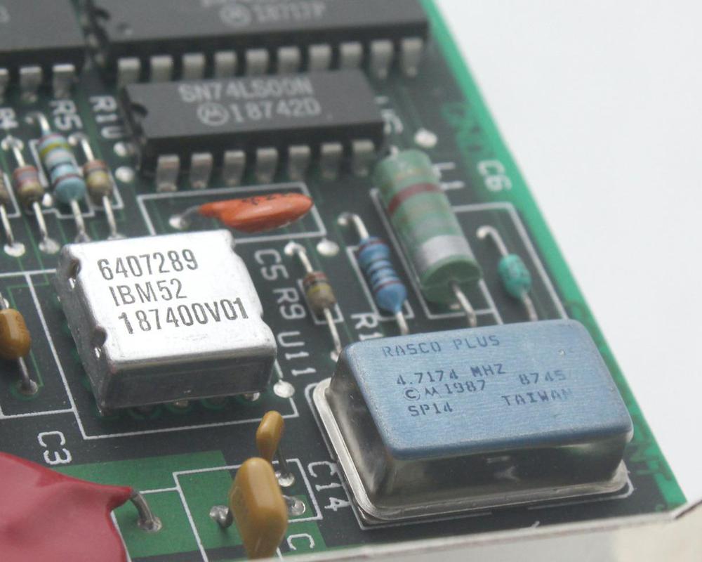
I examined the oscillator module from an IBM PC card.2 The module is packaged in a rectangular 4-pin metal can that protects the circuitry from electrical noise. (It is the “Rasco Plus” rectangular can on the right, not the square IBM integrated circuit.) This module produced a 4.7174 MHz clock signal, as indicated by the text on the package.

The quartz oscillator module is in the lower right, labeled Rasco Plus. 4.7174 MHZ, © Motorola 1987. The square module is an IBM integrated circuit. Click this (or any other image) for a larger version.
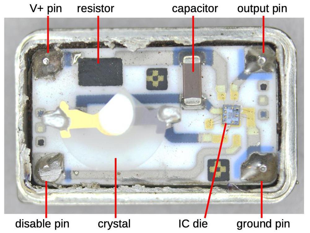
I cut open the can to reveal the hybrid circuitry inside. I was expecting a gem-like quartz crystal inside, but found that oscillators use a very thin disk of quartz. (I damaged the crystal while opening the package, so the upper part is missing..) The quartz crystal is visible on the left, with metal electrodes attached to either side of the crystal. The electrodes are attached to small pegs, raising the crystal above the surface so it can oscillate freely.

Inside the oscillator package, showing the components mounted on the ceramic substrate.
On the right side of the module is a tiny CMOS integrated circuit die. It is mounted on the ceramic substrate and connected to the circuitry by tiny golden bond wires. A surface-mount capacitor (3 nF) and a film resistor (10Ω) on the substrate filter out noise from the power pin.
The IC’s circuitry
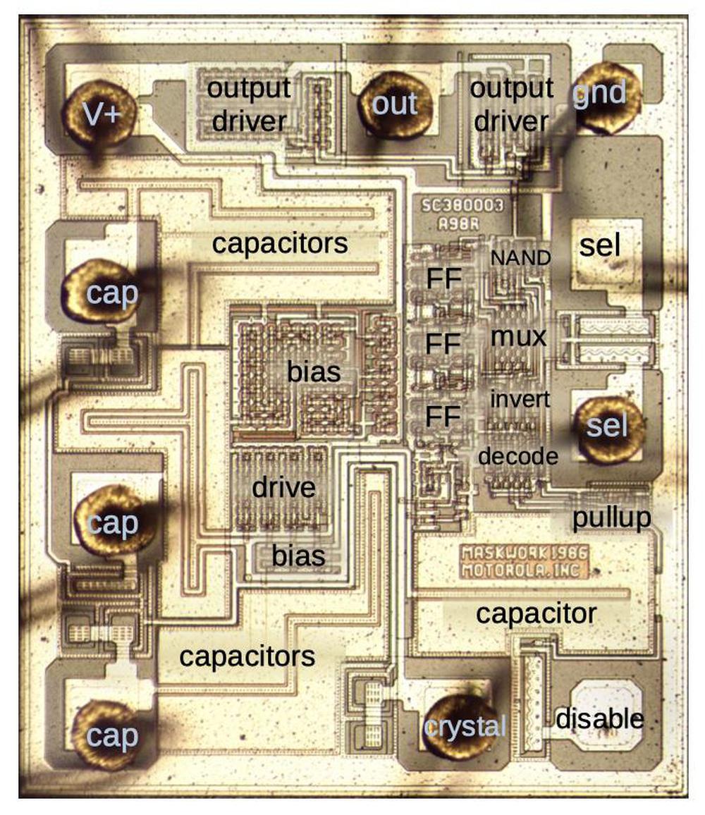
The photo below shows the tiny integrated circuit die under a microscope, with the pads and main functional blocks labeled. The brownish-green regions are the silicon that forms the integrated circuit. A metal layer (yellowish white) wires up the components of the IC. Below the metal, reddish polysilicon implements transistors, but it is mostly obscured by the metal layer. Around the outside of the chip, bond wires are connected to pads, wiring the chip to the rest of the oscillator module. Two pads (select and disable) are left unconnected. The chip was manufactured by Motorola, with a 1986 date. I couldn’t find any information on the part number SC380003.

The integrated circuit die with key blocks labeled. “FF” indicates flip-flops. “sel” indicates select pads. “cap” indicates pads connected to the internal capacitors.
The IC has two functions. First, its analog circuitry drives the quartz crystal to produce oscillations. Second, the IC’s digital circuitry divides the frequency by 1, 2, 4, or 8, and produces a high-current clock output signal. (The division factor is selected by the two select pins on the IC.)
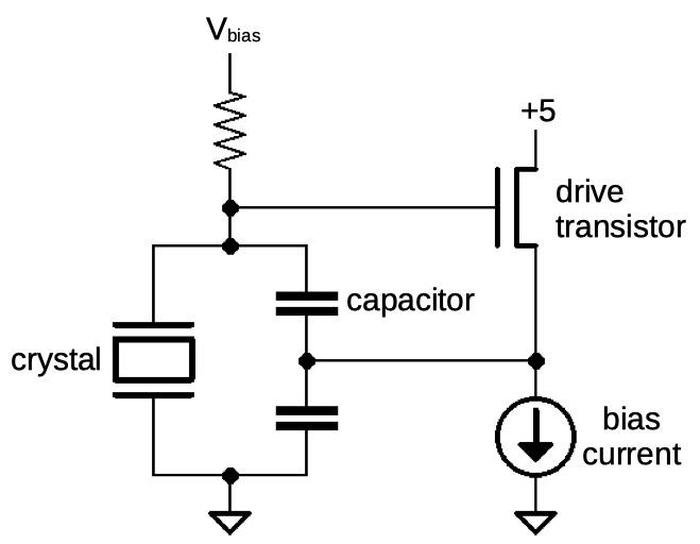
The oscillator is implemented with a circuit (below) called a Colpitts oscillator, which is more complex than the usual quartz oscillator circuit.43 The basic idea is that the crystal and the two capacitors oscillate at the desired frequency. The oscillations would rapidly die out, however, except for the feedback boost from the drive transistor.

Simplified schematic of the oscillator.
In more detail, as the voltage across the crystal increases, the transistor turns on, feeding current into the capacitors and boosting the voltage across the capacitors (and thus the crystal). But as the voltage across the crystal decreases, the transistor turns off and the current sink (circle with arrow) pulls current out of the capacitors, reducing the voltage across the crystal. Thus, the feedback from the drive transistor strengthens the crystal’s oscillations to keep them going.
The bias voltage and current circuits are an important part of this circuit. The bias voltage sets the drive transistor’s gate midway between “on” and “off”, so the voltage oscillations on the crystal will turn it on and off. The bias current is set midway between the drive transistor’s on and off currents so the current flowing in and out of the capacitors balances out.5 (I’m saying “on” and “off” for simplicity; the signal will be a sine wave.)
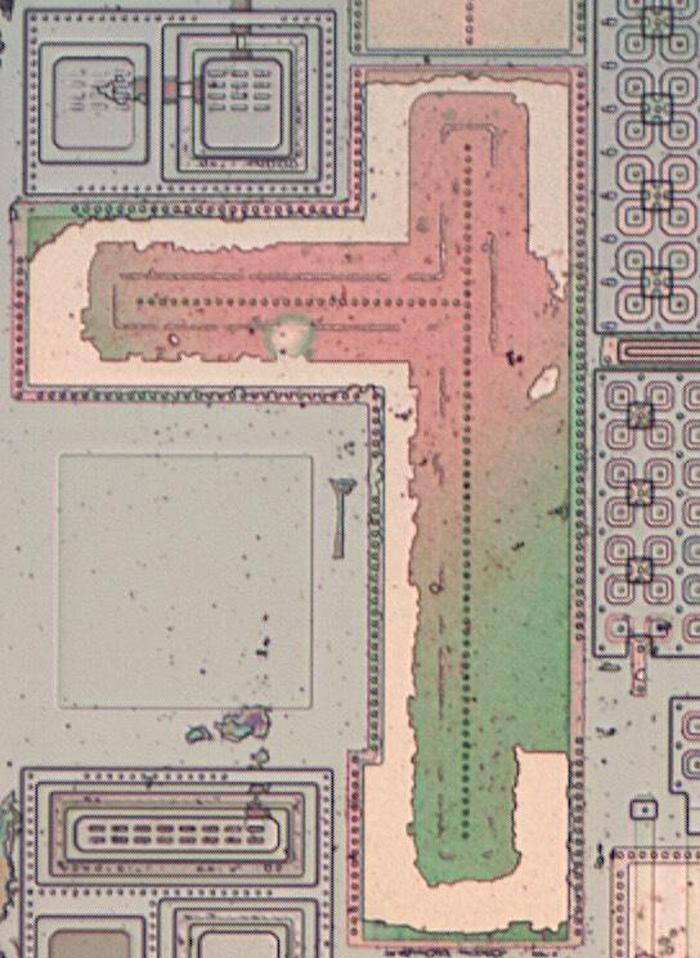
A large part of the integrated circuit is occupied by five capacitors. One is the upper capacitor in the schematic, three are paralleled to form the lower capacitor in the schematic, and one stabilizes the voltage bias circuit. The die photo below shows one of the capacitors after dissolving the metal layer on top. The red and green region is polysilicon, which forms the upper plate of the capacitor, along with the metal layer. Underneath the polysilicon, the pinkish region is probably silicon nitride, forming the insulating dielectric layer. The doped silicon (not visible underneath) forms the bottom plate of the capacitor.

A capacitor on the die. The large faint square to the left of the capacitor is a pad for connecting a bond wire to the IC. The complex structures on the left are clamp diodes on the pins. The cloverleaf structures on the right are transistors, which will be discussed later.
Curiously, the capacitors aren’t connected together on the chip, but are connected to three pads that are wired together by bond wires. Perhaps this provides flexibility; the capacitance in the circuit can be modified by omitting the wire to a capacitor.
The digital circuitry
The right side of the chip contains digital circuitry to divide the crystal’s output frequency by 1, 2, 4, or 8. This lets the same crystal provide four different frequencies. The divider is implemented by three flip-flops in series. Each one divides its input pulses by 2. A 4-to-1 multiplexer selects between the original clock pulses, or the output from one of the flip-flops. The choice is made through the wiring to the two select pads on the right side of the die, fixing the ratio at manufacturing time. Four NAND gates (along with inverters) are used to decode these pins and generate four control signals to the multiplexer and flip-flops.
How CMOS logic is implemented
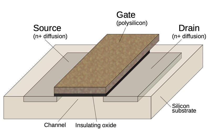
The chip is built with CMOS logic (complementary MOS), which uses two types of transistors, NMOS and PMOS, working together. The diagram below shows how an NMOS transistor is constructed. The transistor can be considered a switch between the source and drain, controlled by the gate. The source and drain (green) consist of regions of silicon doped with impurities to change its semiconductor properties and called N+ silicon. The gate consists of a special type of silicon called polysilicon, separated from the underlying silicon by a very thin insulating oxide layer. The NMOS transistor turns on when the gate is pulled high.

Structure of an NMOS transistor. A PMOS transistor has the same structure, but with N-type and P-type silicon reversed.
A PMOS transistor has the opposite construction from NMOS: the source and drain consist of P+ silicon embedded in N silicon. The operation of a PMOS transistor is also opposite from the NMOS transistor: it turns on when the gate is pulled low. Typically PMOS transistors pull the drain (output) high, while NMOS transistors pull the drain low. In CMOS, the transistors act in a complementary fashion, pulling the output high or low as needed.
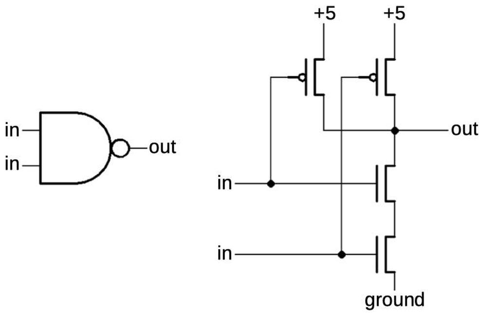
The diagram below shows how a NAND gate is implemented in CMOS. If an input is 0, the corresponding PMOS transistor (top) will turn on and pull the output high. But if both inputs are 1, the NMOS transistors (bottom) will turn on and pull the output low. Thus, the circuit implements the NAND function.

A CMOS NAND gate is implemented with two PMOS transistors (top) and two NMOS transistors (bottom).
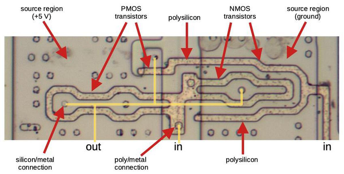
The diagram below shows how a NAND gate appears on the die. The transistors have complex, meandering shapes, unlike the rectangular layouts that appear in textbooks. The left side holds the PMOS transistors, while the right side holds the NMOS transistors. The polysilicon that forms the gates is the slightly reddish wiring on top of the silicon. Most of the underlying silicon is doped, making it conductive and slightly darker than the non-conductive undoped silicon along the left and right edges and in the center. For this photo, the metal layer was removed with acid to reveal the silicon and polysilicon underneath; the yellow line illustrates where some of the metal wiring was. The circles are connections between the metal layer and the underlying silicon or polysilicon.

A NAND gate as it appears on the die.
The transistors in the die photo can be matched up with the NAND-gate schematic; look at the transistor gates formed by polysilicon and what they separate. There is a path from the +5 region to the output through the large elongated PMOS transistor on the left, and a second path through the small PMOS transistor near the center, indicating the transistors are in parallel. Each gate is controlled by one of the inputs. On the right, a path from ground to the output connection must go through both of the concentric NMOS transistors, indicating they are in series.
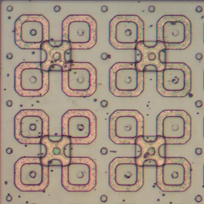
This integrated circuit also uses many circle-gate transistors, an unusual layout technique that allows multiple transistors in parallel at high density. The photo below shows 16 circle-gate transistors. The copper-colored cloverleaf patterns are the transistor gates, implemented with polysilicon. The inside of each “leaf” is the transistor drain, while the outside is the source. The metal layer (removed) wires all the sources, gates, and drains together respectively; the parallel transistors act as one larger transistor. Paralleled transistors are used in the output pin drivers to provide high current for the output. In the bias circuitry, different numbers of transistors are wired together (e.g. 6, 16, or 40) to provide the desired current ratios.

Sixteen circle-gate transistors with four gate connections.
Transmission gate
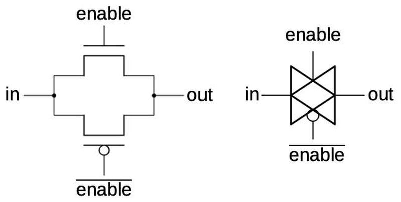
Another key circuit in the chip is the transmission gate. This acts as a switch, either passing a signal through or blocking it. The schematic below shows how a transmission gate is constructed from two transistors, an NMOS transistor and a PMOS transistor. If the enable line is high, both transistors turn on, passing the input signal to the output. If the enable line is low, both transistors turn off, blocking the input signal. The schematic symbol for a transmission gate is shown on the right.

A transmission gate is constructed from two transistors. The transistors and their gates are indicated. The schematic symbol is on the right.
Multiplexer
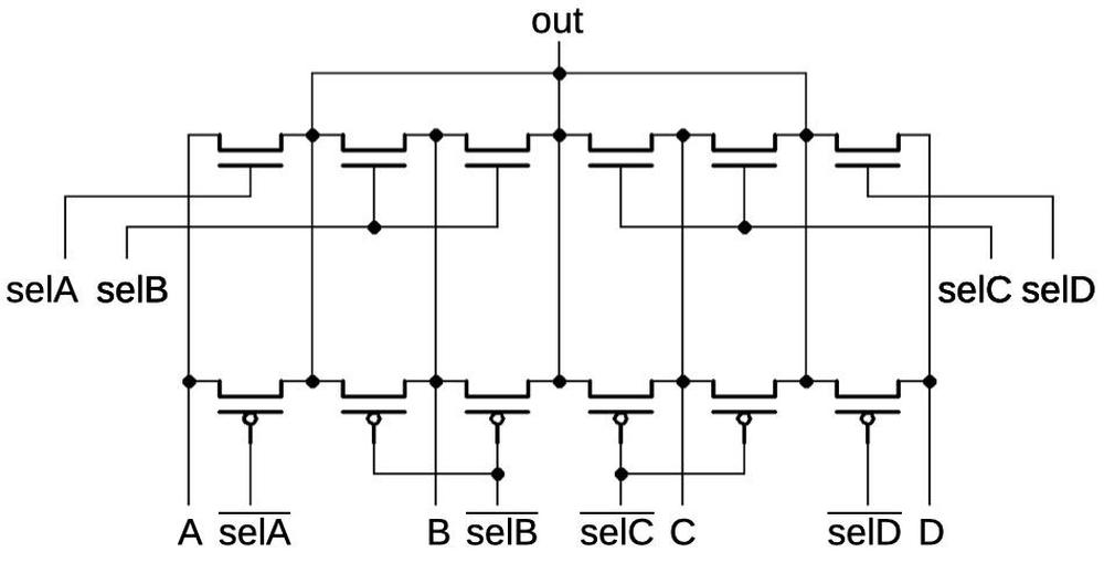
A multiplexer is used to select one of the four clock signals. The diagram below shows how the multiplexer is implemented from transmission gates. The multiplexer takes four inputs: A, B, C, and D. One of the inputs is selected by activating the corresponding select line and its complement. That input is connected through the transmission gate to the output, while the other inputs are blocked. Although a multiplexer can be built with standard logic gates, the implementation with transmission gates is more efficient.

The 4-to-1 multiplexer is implemented with transmission gates.
The schematic below shows the transistors that make up the multiplexer. Note that inputs B and C have pairs of transistors. I believe the motivation is that a pair of transistors presents half the resistance to the signal. Since inputs B and C are the higher-frequency signals, the pair of transistors allows them to pass through with less distortion and delay.

Schematic of the multiplexer, matching the physical layout on the chip.
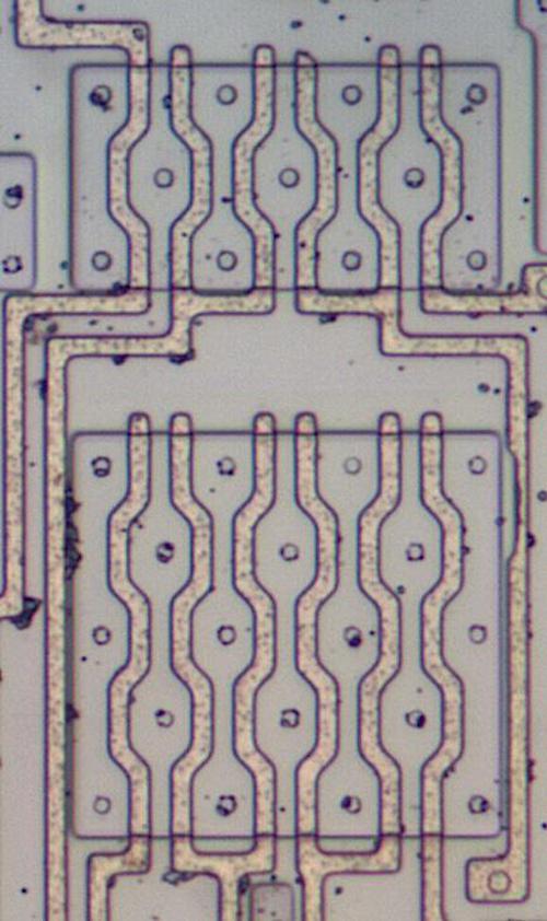
The image below shows how the multiplexer is physically implemented on the die. The polysilicon gate wiring is most prominent. The metal layer has been removed; the metal lines ran vertically connecting corresponding transistors segments. Note that the sources and drains of neighboring transistors are merged into single regions between the gates. The top rectangle holds the NMOS transistors while the lower rectangle holds the PMOS transistors; because PMOS transistors are less efficient, the lower rectangle needs to be larger.

Die photo of the multiplexer.
Flip-flop
The chip contains three-flip-flops to divide the clock frequency. The oscillator uses toggle flip-flops, that flip between 0 and 1 each time they receive an input pulse. Since two input pulses result in one output pulse (0→1→0), the flip-flop divides the frequency by 2.
A flip-flop is constructed from transmission gates, inverters, and a NAND gate, as shown in the schematic below. When the input clock is high, the output passes through the inverter and the first transmission gate to point A. When the input clock switches low, the first transmission gate opens, so point A holds its previous value. Meanwhile, the second transmission gate closes, so the signal passes through the second inverter and transmission gate to point B. The NAND gate inverts it again, causing the output to flip from its previous value. A second cycle of the input clock repeats the process, causing the output to return to its initial value. The result is that two cycles of the input clock result in one cycle of the output, so the flip-flop divides the frequency by 2.

Implementation of a toggle flip-flop.
Each flip-flop has an enable input. If a flip-flop is not needed for the selected output, it is disabled. For instance, if the “divide by 2” mode is selected, only the first flip-flop is used, and the other two are disabled. I assume this is done to reduce power consumption. Note that this is independent from the module’s disable pin, which blocks the module output entirely. This disable feature is optional; this particular module does not provide the disable feature and the disable pin is not wired to the IC.
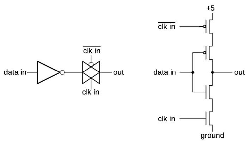
The schematic above shows the inverters and transmission gates as separate structures. However, the flip-flop uses an interesting gate structure that combines the inverter and the transmission gate (left) into a single gate (right). The pair of transistors connected to data in function as an inverter. However, if the clock in is low, both power and ground are blocked so the gate will not affect the output and it will hold its previous voltage. This provides the transmission gate functionality.

Implementation of a combination inverter / transmission gate.
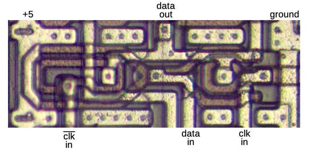
The photo below shows how one of these gates appears on the die. This photo includes the metal layer on top; the reddish polysilicon gates are visible underneath. The two PMOS transistors are on the left, as concentric loops, while the NMOS transistors are on the right.

One of the combination inverter / transmission gates, as it appears on the die.
Conclusion
While the oscillator module looks simple from the outside, on the inside there’s a lot more complexity than you might expect.6 It contains not just a quartz crystal but also discrete components and a tiny integrated circuit. The integrated circuit combines capacitors, analog circuitry to drive the oscillations, and digital circuitry to choose a frequency. By changing the wiring to the integrated circuit during manufacturing, four different frequencies can be selected.
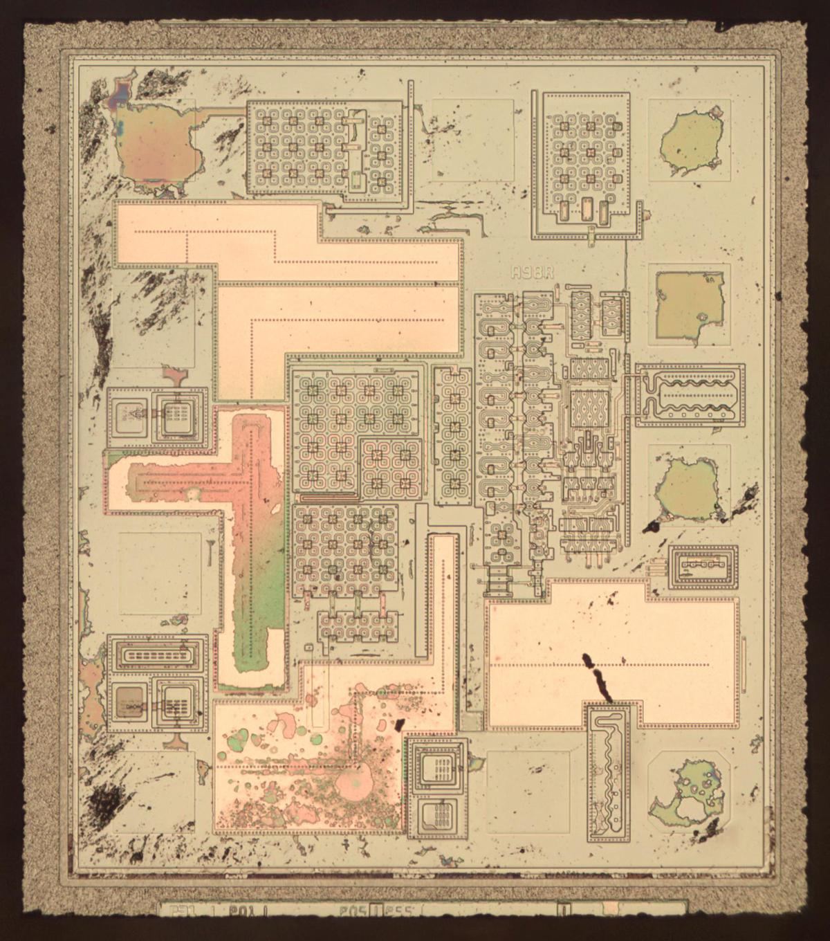
I’ll end with the die photo below showing the chip after removing the metal and oxide layers, showing the silicon and polysilicon underneath. The large pinkish capacitors are the most visible feature in this image, but the transistors can also be seen. (Click the image for a larger version.)

Die photo of the oscillator chip with metal removed to show the polysilicon and silicon underneath.
I announce my latest blog posts on Twitter, so follow me at kenshirriff. I also have an RSS feed.
Notes and references
